- FPC[6]
- Other PCB & PCBA[10]
- Single-Sided PCB[10]
- Electrical Ceramics[1]
- Rigid PCB[8]
- Multilayer PCB[6]
- Contact Person : Mr. wu Jackie
- Company Name : Shenzhen Great Electronics Co., Ltd.
- Tel : 86-755-33578889
- Fax : 86-755-81760186
- Address : Guangdong,Shenzhen,Rm 407 4F, 10-12F, 1-5F, Xinghe Building, Shajing Street, Bao'an District, Shenzhen City, China
- Country/Region : China
- Zip : 518125
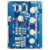
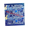
FR4 double-sided pcb IC bonding board
1. FR4 material,1oz copper, board thickness 1.6mm2. blue ink solder mask, IC bonding pcb
3. Fast delivery time,with competitive price
4. Certificate: ROHS, UL, ISO9001-2000, ISO14001
Our Manufacturing Capability for PCB Board
1). Material type: CEM-3,FR-4,FR-4-TG170/TG180,Halogen Free,Rogers,Arlon,Taconic,Isola,PTFE, Bergquist
2). Surface Treatment: HASL,HASL lead-free,HAL,Flash gold,immersion gold,OSP,Gold Finger Palting,Selective thick gold plating, immersion silver,immersion tin, Carbon ink,peelable mask
3). Solder mask colour: Green/MATT Green/Blue/Yellow/White/Black/Red
4). Board Size: 650mm*1000mm
5). Board Layer: 1L-26L
6). Board thickness: 0.2mm to 6.0mm
7). Finished Copper thickness: 0.5 OZ to 6 OZ
8). Min. drilled hole size: 3mil (0.075mm)
9). Min. Line width/Line spacing: 3mil/3mil
10). Copper thickness in hole: >20um
11). Board thickness tolerance: ±10%
12). Outline tolerance: Routing:±0.1mm,Punching:±0.1mm
13). Hole tolerance: PTH: ±0.076mm , NPTH: ±0.05mm
14). impedance control tolerance: ±10%
15). Warp and Twist: <0.75%
16). Tested by:Flying-Probe Tester, Fixture tester , Visual Inspection
17). Special requirements: Buried and blind vias, impedance control, thick Cu PCB,selectivity plating gold 30 microinch
18). Profiling: Punching, Routing, V-CUT, Beveling
19). Certificate: UL,ISO 9001,ISO14001,ROHS
20). We have a sound quality management system,Ensure the quality of all products
Low cost (100USD) Prototype PCB:
Qty: 10pcs
Board size: 100mm*150mm
Layers: Double-sided
Material: FR4 or AL
Board thickness: 1.6mm
Copper thickness: 1oz
Surface finished: HASL lead-free
Lead time: 5 working days
Prototype for standard process specification
Fast Prototype:
24-hour for 2L PCB
48-hour for 4L PCB
72-hour for 6L and 8L PCB
120-hour for 10L or more layers PCB at the soonest
FR4 double-sided pcb IC bonding board


